
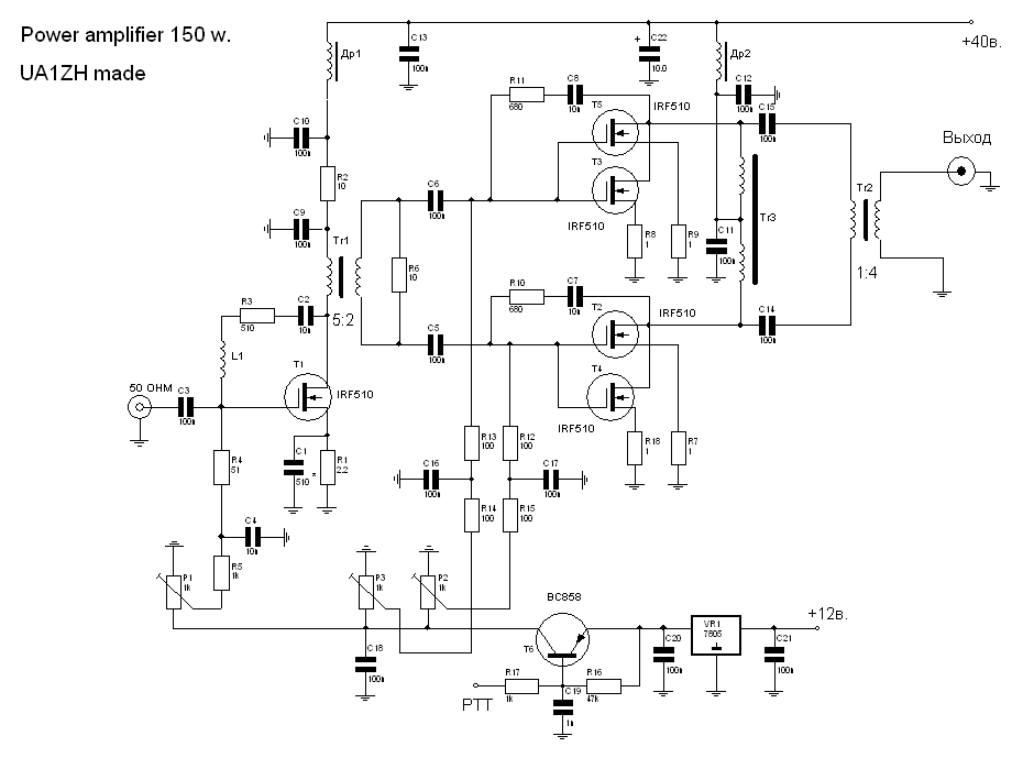
NTC resistor as a protection study
Obviously adding a NTC resistor as a protection and compensator against Thermal runaway is something i was consisdering initially . I did some test with different value for NTC (From 1K up to 5K).
The system is reacting really well against thermal runaway , therefore is really too sensitive and the Biasing voltage was fluctuating too much and too quickly in a magnitude range of 3.7vdc down to 1 or 2vdc . This swing is involving very quickly a terrible modulation and really bad IMD3. The protection was really efficient but the modulation and amplifier efficiency were really fuzzy and not consistent.
In fact the main difficulty with NTC is where to install it . Too close from the MOSFET , the temperature will climb to fast and away from the MOSFET the temperature will rise too slowly.
Using diodes instead are less sensitive and the Bias Voltage swing is better without any IMD3
Уникальные характеристики Irf530n
Irf530n — это мощный N-канальный полевой транзистор, который имеет ряд уникальных характеристик.
- Низкое входное сопротивление: Irf530n обладает очень низким входным сопротивлением, что позволяет ему эффективно управлять большими токами в схемах регулирования напряжения.
- Высокая мощность: благодаря своей конструкции Irf530n может работать с высокими уровнями тока и мощности, что делает его идеальным для использования в мощных регуляторах напряжения.
- Широкий диапазон рабочих напряжений: Irf530n способный работать с широким диапазоном напряжений, что позволяет его использование в различных электронных устройствах.
- Отличные электрические характеристики: этот полевой транзистор обладает низким уровнем шума, низкой температурной зависимостью и высоким коэффициентом усиления. Эти факторы делают его надежным и эффективным при использовании в схемах регулирования напряжения.
В целом, Irf530n является высококачественным полевым транзистором с уникальными характеристиками, которые делают его привлекательным для использования в схемах регулирования напряжения.
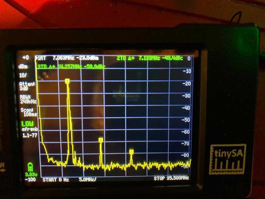
Spectral purity
This is the spectral purity 2 tones and 25w output
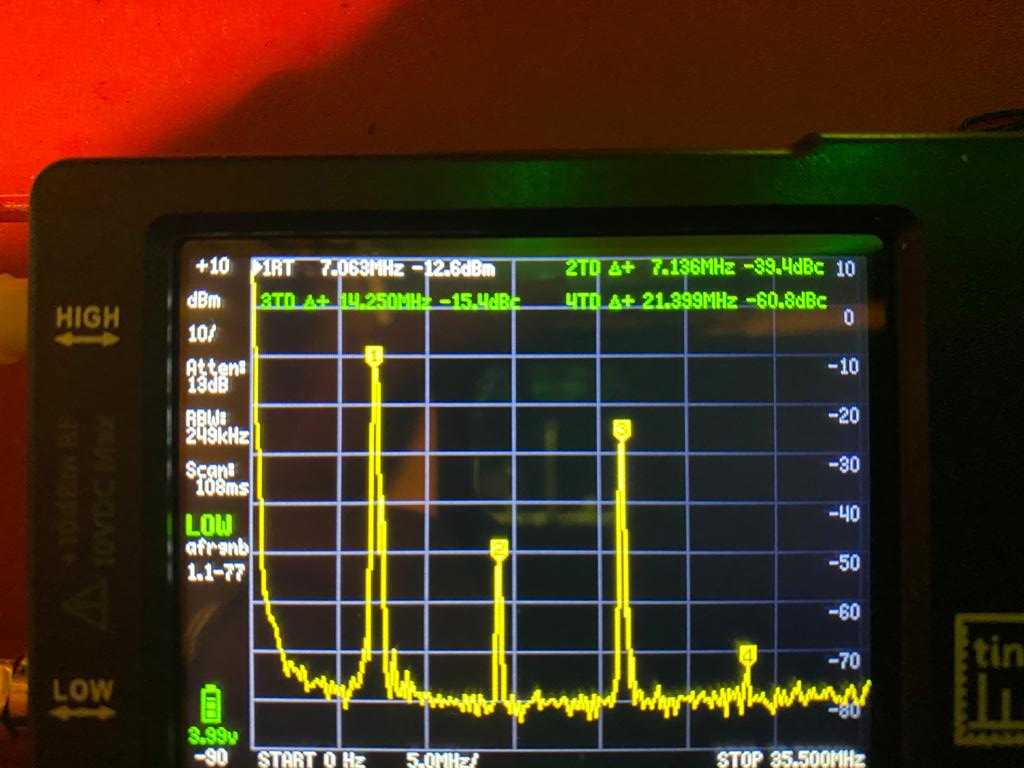
A quick check without the LPF
Important
IRF530 Mosfet are not dedicated for HF usage and according with that it is not realistic to provide more than 30W with 2 IRF530 without producing significant spurious ,IMD and 2nd/3rd Order harmonics at the suitable level means < -50dB.
Feeding with more than 14vdc the IRF530 is working but the MOSFET will not sustain such voltage due to Thermal Runaway (The temperature and current may increase and will be difficult to control) . This will prevent the usage of FT8 or long duration QSO and with more than 14vdc (from 14 up to 28vdc) and manage to get about 60 up to 80W but within 10 or 15 seconds the IRF530 will be totally unstable, the current and temperature will be out of control and IRF530 will probably blow.
The drain and Gate voltage should be provided ith a current limiting system in order to protect against any current overloading and Thermal runaway (See below the thermal regulation protection).
I will have the same comment regarding the biasing and exceeding 40ma or 100ma overall and 3.7vdc will provide also a totally unstable transistor after few seconds with the same result : Transistor blow
In addition a voltage above 14 Vdc and a biasing current above 40ma (100ma overall) are providing significant IMD and the spectral purity is not good at all. 40ma (One transistor) biasing is in my point of vue the maximum current in order to achieve a compliant spectral purity
The maximum input power for 2 IRF530 without attenuator is 1.5 to 2w , otherwise the spurious or IMD will transform your spectral analyzer screen into a Xmas Tree. With 0.5 up to 1 w i manage to have 40 to 45w output which is i was targeting.
For my amplifier the drain voltage for the mosfet is about 13.5vdc with a 40ma biasing current and 3.7vdc for the gate. i can run this amplifier permanently for one hour without any issue and the spurious/spectral purity are acceptable (My biasing current is about 60ma overall) . I use this amplifier with this setup for months now without any problem. Needless to say that you need to apply a proper cooling system with a radiator and a fan.
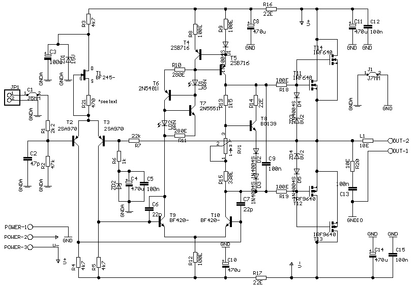
Biasing (quiescent current)
The quiescent operation point will Influence the gain of the transistor, and change theoutput waveform (linearity) and spectral purity.
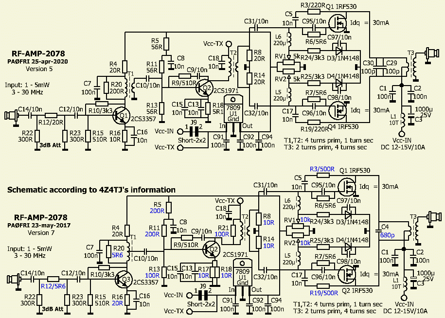
The Quiescent current you should target is 20ma up to 40ma (for one IRF530 means about 40ma up to 80ma for a pair of IRF530) is the magnitude you should target and you need to replace the R7 resistor with a 220R to achieve this result. The biasing voltage is about 3.5Vdc up to 3.7Vdc. In order to achieve this correct biasing (40 up to 80ma for 2 IRF530), R7 and VR1 resistor are important and should be adjusted with different value in order to provide the suitable biasing (3.7v and 40ma max). One thing very important and i notice the biasing should be adjusted according the pair IRF530 you are using . My setup is about 3.73vdc in order to achieve a perfect modulation and a great spectral purity . In accordance you should pay a special attention for the biasing setup with this kind of Mosfet . To provide you an example during my test initially i was using the stock IRF530 provided with the kit and my initial biasing was about 2.5 up to 2.7vdc for a great biasing . After blowing my mosfet during many test and obviously some mistakes i swap with new IRF530 and my initial setup with 2.7vdc was simply terrible , providing a terrible AF (modulation) quality and spurious with a terrible spectral purity . With the new IRF530 my final setup is finally 3.7vdc with 60ma current . I am using this setup for more than one year and this amplifier is running really like a charm with a great modulation and a good spectral quality.


Achievements
The main extent for an Amateur radio is to build , experiment , setup and use its own build equipement . Using IRF530 transistors is a challenge since this MOSFET is not designated to be used as a HF Linear Amplifier (It was the same regarding my EL519 Tube amplifier). The main challenge is to achieve a great device especially for amplifier with a good spectral purity and make it compliant. I spent hours , blow (Few blow was like a gunshot!!!!) about 15 transistors (Surely more hahahahaha !!!!!) but at the end of the road the result is great.
I am running this amplifier for 3 years now without a single glitch or issue and use it mostly for Digital modes likely PSK31, RTTY and FT8 but also for CW QSO.
Obviously the IRF530 is not the best choice and best performer , therefore with some patience and testing you can achieve a very decent and cheap tiny amplifier. As mentioned above building this kind of amplifier using IRF530 is a cheap and easy introduction for newbies. The IRF530 is tricky and you will learn a lot about capacitance (Especially at the input for the IRF530), biasing , quiescent current , IMD ans spectral purity. It will be a great introduction for LDMOS amplifier
Some details regarding the IRF530 Amplifier:
Описание полевого транзистора IRF530
- Напряжение стока до 100 В
- Силовая мощность до 100 Вт
- Сопротивление стока-истока до 0,16 Ом
- Ток стока до 14 А
IRF530 обладает высокой производительностью благодаря своей конструкции и использует технологию MOSFET. Он имеет низкое сопротивление стока-истока и высокую эффективность, что делает его идеальным для многих применений.
Транзистор IRF530 обычно используется в схемах управления мощными нагрузками, такими как электромоторы, освещение и источники питания. Он может быть использован в схемах постоянного и переменного тока. Благодаря своим характеристикам, IRF530 может эффективно контролировать высокие токи и напряжения, обеспечивая стабильную и надежную работу системы.
Datasheets
Datasheet
PDF, 101 Кб
Выписка из документа
Philips Semiconductors Product specification N-channel TrenchMOSTM transistor IRF530N FEATURES ‘Trench’ technology Low on-state resistance Fast switching Low thermal resistance SYMBOLd QUICK REFERENCE DATA VDSS = 100 V ID = 17 Ag RDS(ON) 110 ms GENERAL DESCRIPTIONN-channel enhancement mode field-effect power transistor in a plastic envelope using ‘trench’ technology. Applications: d.c. to d.c. converters switched mode power supplies The IRF530N is supplied in the SOT78 (TO220AB) conventional leaded package. PINNINGPIN 1 2 3 tab gate drain source drain DESCRIPTION SOT78 (TO220AB)tab drain 1 2 3 gate source drain LIMITING VALUESLimiting values in accordance with the Absolute Maximum System (IEC 134) SYMBOL PARAMETER VDSS VDGR VGS ID IDM PD Tj, Tstg Drain-source voltage Drain-gate voltage Gate-source voltage Continuous drain current Pulsed drain current Total power dissipation Operating junction and storage temperature CONDITIONS Tj = 25 °C to 175°C Tj = 25 °C to 175°C; RGS = 20 k Tmb = 25 °C; VGS = 10 V Tmb = 100 °C; VGS = 10 V Tmb = 25 °C Tmb = 25 °C MIN. -55 MAX. 100 100 ± 20 17 12 68 79 175 UNIT V V V A A A W °C AVALANCHE ENERGY LIMITING VALUESLimiting values in accordance with the Absolute Maximum System (IEC 134) SYMBOL PARAMETER EAS Non-repetitive avalanche energy Peak non-repetitive avalanche current CONDITIONS Unclamped inductive load, IAS = 7.8 A; tp = 300 µs; Tj prior to avalanche = 25°C; VDD 25 V; RGS = 50 ; VGS = 10 V; refer to fig:14 MIN. MAX. 150 UNIT mJ IAS -17 A August 1999 1 Rev 1.100 Philips Semiconductors Product specification N-channel TrenchMOSTM transistor IRF530N THERMAL RESISTANCESSYMBOL PARAMETER Rth j-mb Rth j-a Thermal resistance junction to mounting base Thermal resistance junction to ambient CONDITIONS MIN. SOT78 package, in free air TYP. MAX. UNIT 60 1.9 K/W K/W ELECTRICAL CHARACTERISTICSTj= 25°C unless otherwise specified SYMBOL PARAMETER V(BR)DSS VGS(TO) RDS(ON) gfs IGSS IDSS Qg(tot) Qgs Qgd td on tr td off tf Ld Ld Ls Ciss Coss Crss Drain-source breakdown voltage Gate threshold voltage Drain-source on-state resistance Forward transconductance Gate source leakage current Zero gate voltage drain current Total gate charge Gate-source charge Gate-drain (Miller) charge Turn-on delay time Turn-on rise time Turn-off delay time Turn-off fall time Internal drain inductance Internal drain inductance Internal source inductance Input capacitance Output capacitance Feedback capacitance CONDITIONS VGS = 0 V; ID = 0.25 mA; Tj = -55°C VDS = VGS; ID = 1 mA Tj = 175°C Tj = -55°C VGS = 10 V; ID = 9 A Tj = 175°C VDS = 25 V; ID = 9 A …
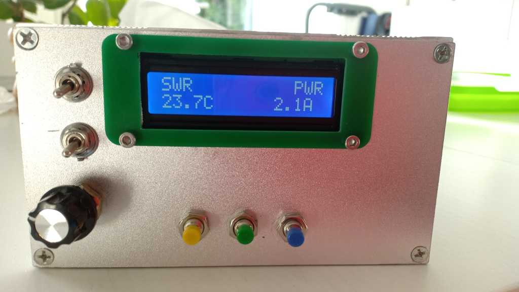
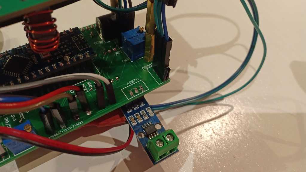
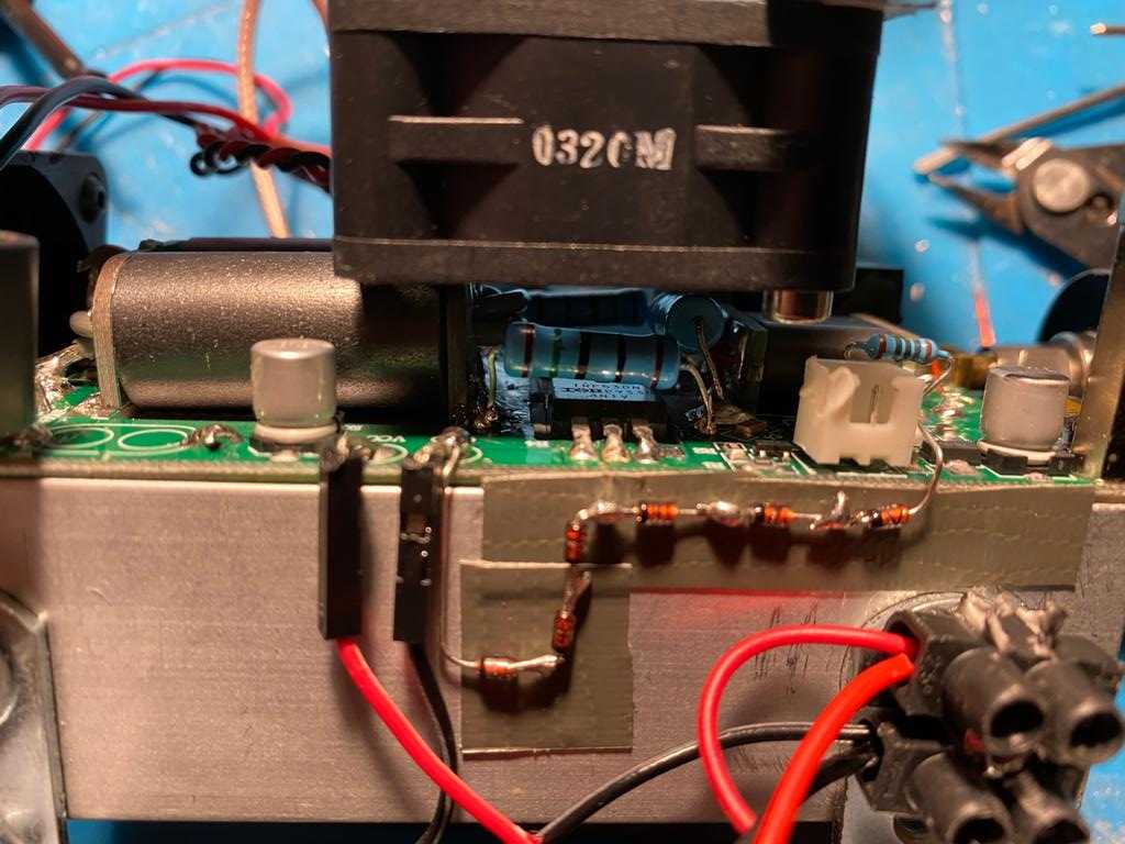
Amplifier Controller
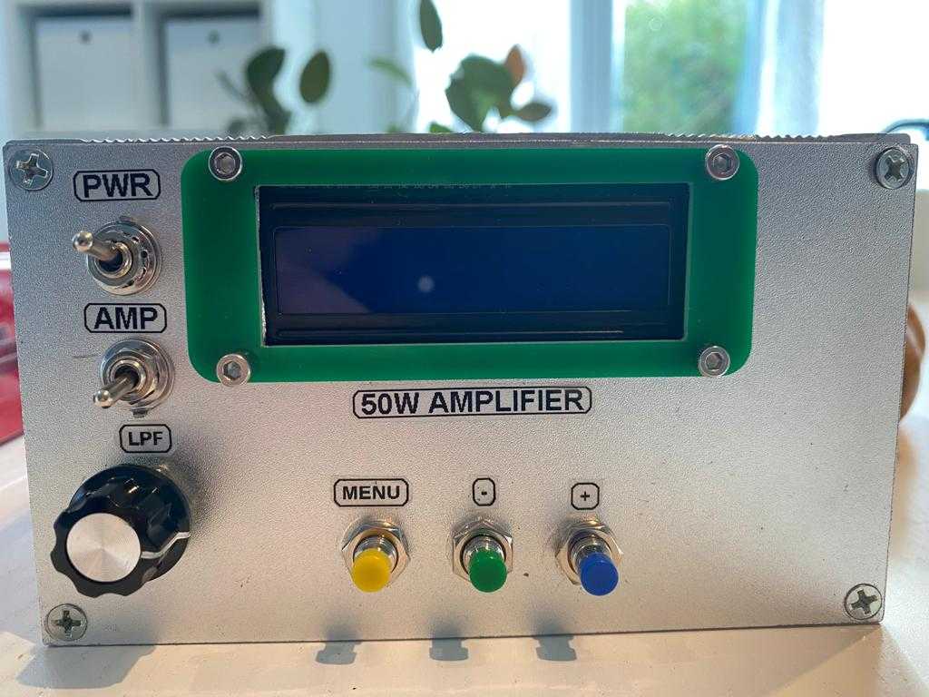
The controller is monitoring the amplifier current and obviously the SWR and output power
- The amplifier is biased with 3.7vdc with about 70ma quiescent current –> input power is 1w for about 40 up to 55w output.
- The controller is providing the following capabilites:
- Temperature monitoring with dedicated menu to adjust the threshold to trigger a 12vdc Fan
- Current monitoring with a dedicated menu to adjust the max amp (Limitation) in order to cut-off the biasing with an opto relay when the current is too high
- A dedicated menu for the Max SWR adjusment –> It will trigger the opto relay to cut-off the biasing
- A dedicated menu to adjust the output power range you want to monitor . Since the power is about 50w , my adjusment is 100w which is tailoring the bargraph display accordingly.
- Using FT50-43 toroids and 5w 50ohm resistor, the SWR bridge able to handle up to 1Kw
The full package : Gerber , BOM, kicad , pictures, and arduino Sketch for the main controller and the SWR bridge : https://drive.google.com/file/d/1OAA3AwHDP3Jk_RUIIhog9YnVMdybFQ75/view?usp=sharing
The Arduino Sketch : https://drive.google.com/file/d/1E4R0gcUoR4Z5WwKWr_Zc6-ottOrRJNIo/view?usp=sharing
Currently i am using MOSFET amplifier for 3 years with this kind of controller with another amplifier and working perfectly.
 before the labelling process
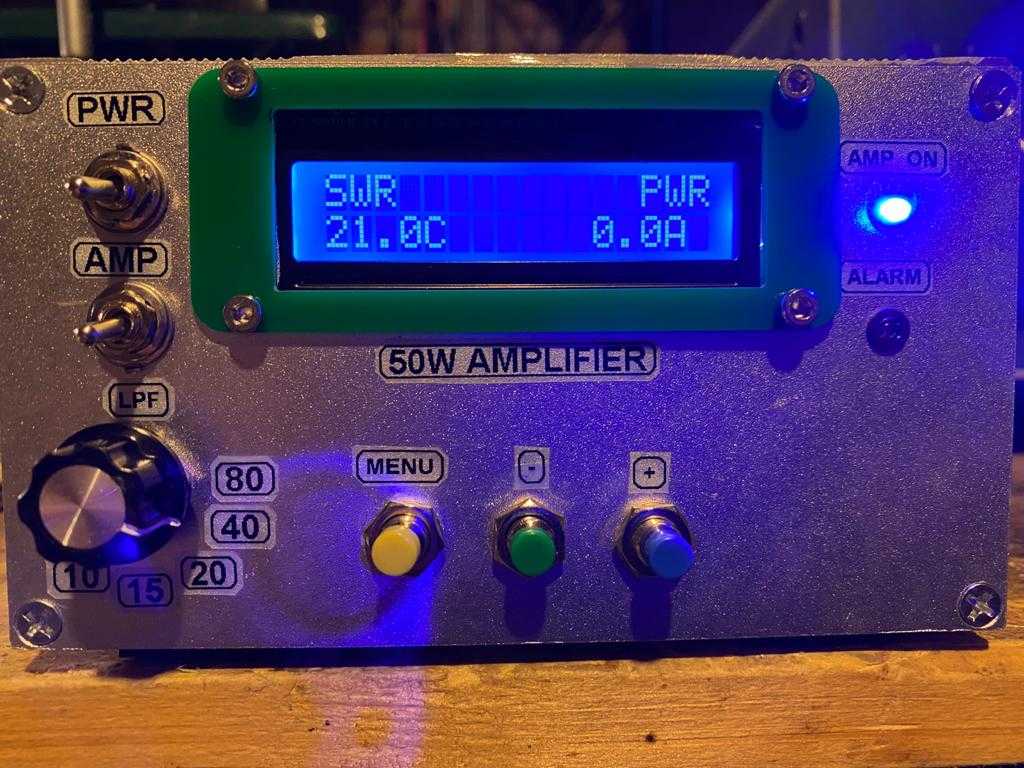
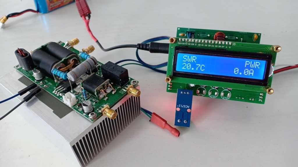
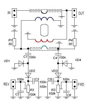
For VD Diodes , i am using BAT41 diodes or 1N5711 . For R1 and R4 since i do not have 50R Resistor , i am using 47R 5w resistor . The Menu is offering to adjust the Resistor Value.
The Toroid core is a ft-80-43 or 140:43 with about 30 turns (The size of your toroid is according the power you are using)
The gerber file for the SWR bridge : https://drive.google.com/file/d/1i1FAbeb4EyGl6EbUAo1TmMHviFV_yVLi/view?usp=sharing
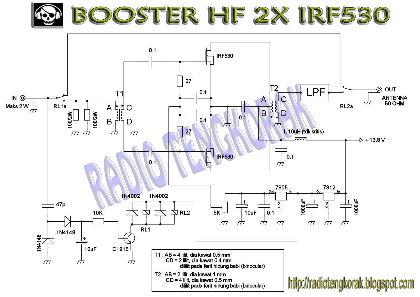


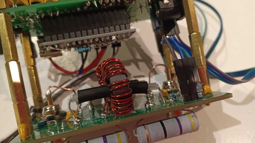
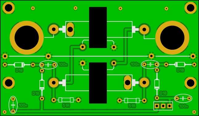
Thermal Protection principle
As mentioned above , the main issue according the IRF530 is the Thermal Runaway involving a catastrophic avalanche effect. The biasing current is usually setup at about 40 up to 50 ma for 2 x IRF530. When running the amplifier few minutes or even seconds , you will notice a significant increase of the Biasing current to few hundreds of ma and you can reach about 1 amp. When getting hotter the internal resistance is rising also . The main result is the mosfet blow out and destruction (gate/source junction). The issue is also notice with Quiescent current when no RF is applied to the gate . the Drain current current could also increase on its own and involving a catastrophic domino or avalanche effect with same the destruction of the Mosfet Source junction especially when the MOSFET is already hot. So with this kind of MOSFET we need to tackle 2 issues
To avoid this issue , there is a simple circuit you should add in the biasing path in order to regulate the biasing current against Thermal Runaway . The biasing is coming from the IC1 7805 Regulator and the thermal regulation is achieve with 1N4148 silicium diodes . The main property of this kind of diode = The current decrease , when the temperature increase. This addon is providing a temperature compensated biasing and protection
The diodes shall be connected to R7 resistor , the cathode to the ground and tackle against the radiator or against one of the MOSFET (This kind of system is widely use with pro amplifier)
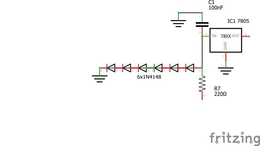
For a better thermal transfer you can put some liquid tape or thermal paste to ensure they are not moving
With this system i can run the amplifier for few minutes without any issue and since my radiator is not so big , after few minutes due to the radiator heat , the biasing current is dropping significantly and the output power is dropping to less than 10watts .
This circuit is also acting as a security for your amplifier and will provide an automatic current regulation regulation for the biasing circuit.
You can install the diodes on the top of the IRF530 casing or very close and fix it with some plastic dip or Sillicone. I did some test and looks like a great solution . The Bias current swing at 45 celcius was not above 100ma. I guess i will implement and test this option very soon.
Применение транзистора Ирф530
Транзистор Ирф530 широко применяется в различных электронных устройствах и системах благодаря своим техническим характеристикам. Ниже предоставлена информация о некоторых областях применения этого транзистора.
1. Источник тока:
- Ирф530 может использоваться в качестве источника постоянного тока, предоставляя стабильное напряжение и текущую нагрузку.
- Он может использоваться для питания различных микросхем, интегральных схем и других электронных компонентов.
2. Усилительный элемент:
- Транзистор Ирф530 может быть использован в качестве усилителя сигнала в радио- и аудиоэлектронике.
- Он может увеличивать амплитуду электронного сигнала, позволяя передавать звуковые и радиочастотные сигналы с нужной мощностью.
3. Ключевой элемент:
- Ирф530 может быть использован в качестве ключевого элемента в различных электронных схемах, где необходимо управление включением и выключением электрического тока.
- Он может использоваться в схемах регулирования яркости светодиодов, управления скоростью электромоторов и других подобных устройствах.
4. Источник питания:
- Транзистор Ирф530 может использоваться в источниках питания для защиты от перенапряжения и короткого замыкания.
- Он способен обеспечивать стабильную работу схем защиты, предотвращая повреждение электронных устройств.
Транзистор Ирф530, благодаря своему набору технических характеристик и возможностей, является универсальным элементом электроники, применяемым в широком спектре устройств и систем.
Recommendations
-For this technology of MOSFET (IRF510, 520 or 530) the maximum input power is 1w for one MOSFET and 1.5 max if using 2 MOSFET . Therefore the best results in terms of spectral purity is with 0.5w up to 1w input.
Building this kind of amplifier for you QRP rig will teach you a lot in terms of spectral purity, IMD , biasing , Fourier Transform, Harmonics and many more . It remains a great experimentation platform and it will provide the basis if you are moving for a more QRO amplifier using LDMOS technology.
If you are using an IRF510 during experimentation with this mosfet i notice, the minimum drain voltage you should use is about 24vdc, 28vdc will be perfect . With 13 up to 22vdc, the IRF510 is a bit unstable with a high impedance at the input and a significant capacitance at the output and will produce IMD and non desirable spurious . Feeding the drain with 28vdc for an IRF510 is providing a stable amplifier with reasonnable spurious.
-Biasing : for IRF530 the maximum idq current is about 30 to 40ma (Voltage will be between 3.5v and 3.7v) and i adjust mine to 3.7vdc for 40ma current. A proper adjustment of the biasing is really the key to achieve a clean amplifier. Never use the the Bias to adjust the output power. A wrong biasing will provide spurious , IMD , modulation clipping and distortion. With an unproper biasing the 2nd/3rd Order harmonics will be non acceptable.
-Thermal Runaway protection is MANDATORY with this kind of MOSFET not only for the Mosfet protection but also for the Spectral purity. With or Without it is day and night.


-A protection controller is highly recommended to protect the Amplifier (SWR, Bias and Gate/drain current/voltage)
-Current limiting circuit for the Drain and Gate voltage is mandatory
-Drain Voltage for IRF530 should not be above 14vdc;
-Gate biasing voltage should not exceed 4v for IRF530 MOSFET (Mine is 3.7vdc)
-Biasing Voltage and current should have about 3.7v with about 40ma current per transistor . My setup is 3.73vdc for about a total of 60ma biasing current.
-A good quality LFP filter is MANDATORY
Without applying the conditions as above , your amplifier will generate non desirable harmonics level and the spectral purity will not fit the FCC rules we should cope as amateur radio in all respects.
This tiny amplifier is really great and cost-effective (14 Euros for a kit). i can use it even for FT8 or RTTY long QSO without any issue. The output power provided is able to drive nicely my 2 EL519 amplifiers and with 18 up to 20w i can achieve about 300w and 600w
I am driving my tube amplifier (EL519) from my SDR transceivers with only 0.5 watts and i get 15 up to 20 watts output from this amplifier. My overall output power including my tube amplifier is about 270 up 310w which is sufficient.