IRF630 POWER MOSFET electrical specification explanation
In this section we try to explain the electrical specifications of IRF630 MOSFET, this description is really helpful for a better understanding of this device.
Voltage specs
The terminal voltage specs of IRF630 MOSFET are the drain to source voltage is 200V, the gate to source voltage is +/-20V, and gate to source threshold voltage is 2V to 4V.
The voltage specifications of IRF630 MOSFET shows that it is a power device which had more power applications.
Current specs
The drain current value IRF630 MOSFET is 9A and the pulsed drain current value is 36A.
The overall current specifications of IRF630 MOSFET show that it is a powerful device that has a driver and switching applications.
Zero gates voltage drain current
The value for zero gate voltage drain current is 25 to 250uA, it is a specific condition where the gate voltage is at zero and the current is a specific value with respect to voltage value.
Dissipation specs
The power dissipation value of IRF630 MOSFET is 74W, the power dissipation capacity of the device shows that it had more applications for power switching and power supply applications.
Total gate charge
The total gate charge value of IRF630 is 43nC, this particular device had a feature which is the minimum gate charge value.
Input capacitance
The input capacitance value of IRF630 MOSFET is 800pF, this MOSFET had a minimum capacitance value compared with other devices.
IRF630 vs IRF740 vs IRF644
In this table, we try to compare the electrical specifications of three MOSFET devices such as IRF630, IRF740, and IRF644, this spec comparison is really helpful for a better understanding of devices.
| Characteristics | IRF630 | IRF740 | IRF644 |
|---|---|---|---|
| Drain to source voltage (VDS)) | 200V | 400V | 250V |
| Gate to source voltage (Vgs) | 20V | 20V | 20V |
| Gate threshold voltage (Vg(th)) | 2 to 4V | 2 to 4V | 2 to 4V |
| Drain current (Id) | 9A | 10A | 14A |
| Pulsed drain current | 36A | 40A | 56A |
| Zero gate voltage drain current (IDSS) | 25 to 250uA | 25 to 250uA | 25 to 250uA |
| Total gate charge (Qg) | 43nC | 63nC | 68nC |
| Power dissipation (PD) | 74W | 125W | 125W |
| Junction temperature (TJ) | -55 to +150°C | -55 to +150°C | -55 to +150°C |
| Drain to source on-state resistance (RDS) | 0.40Ω | 0.55Ω | 0.28Ω |
| Rise time (tr) | 28ns | 27ns | 24ns |
| Reverse recovery time (trr) | 170 to 340ns | 370 to 790ns | 250 to 500ns |
| Input capacitance | 800pf | 1400pf | 1300pf |
| Output capacitance | 240pf | 330pf | 330pf |
| Package | TO-220AB | TO-220AB | TO-220AB |
IRF630 POWER MOSFET specification
- IRF630 is an N-channel POWER MOSFET device
- Drain to source voltage (VDS) is 200V
- Gate to source voltage (VGS) is +/- 20V
- Gate to the threshold voltage (VGS (th)) is 2V to 4V
- Drain current (Id) is 9A
- Pulsed drain current (IDM) is 36A
- Power dissipation (PD) is 74W
- Total gate charge (Qg) is 43nC
- Drain to source on-state resistance (RDS (ON)) 40Ω
- Zero gate voltage drain current (IDSS) is 25 to 250uA
- Rise time (tr) is 28ns
- Peak diode recovery dv/dt is 5V/ns
- Thermal resistance junction to ambient (Rth j-A) is 62℃/W
- Junction temperature (TJ) is between -55 to 150℃
- Body diode reverse recovery (trr) 170 to 340ns
- Input capacitance is 800pf
- Output capacitance is 240pf
- Extremely high dv/dt capacity
- Very low intrinsic capacitance
- Gate charge minimized
- Repetitive avalanche rated
- Fast switching
- Ease of paralleling
- Simple drive requirement
- High efficiency
- Ruggedized device design
- Low on-resistance
- Cost-effectiveness
- Low thermal resistance
Characteristics curves of IRF630 MOSFET
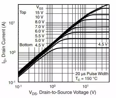
 output characteristics of IRF630 MOSFET
The figure shows the output characteristics of IRF630 MOSFET, the graph is plotted with drain current vs drain to source voltage.
At the different gates to source voltage variations and fixed temperature values, the drain current will increase towards a limit and become constant, this is the happened at all the values.
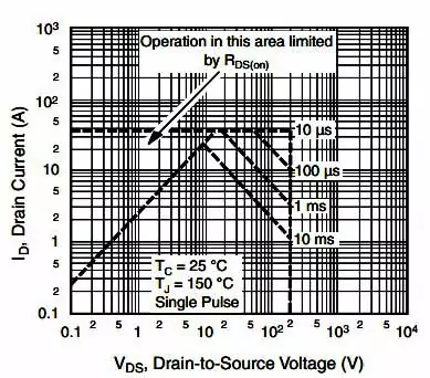
 maximum safe operating area of IRF630 MOSFET
The figure shows the maximum safe operating area of IRF630 MOSFET, the graph plots with different variations such as drain current, drain to source voltage, junction temperature, switching speed, and on-state resistance.
From the graph we can see different variations of IRF630 MOSFET, so we can use this data for different applications.


