
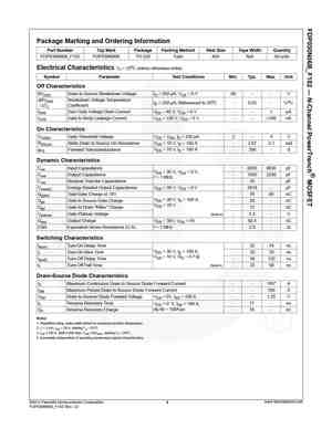
FDP030N06 Datasheet (PDF)
1.1. fdp030n06.pdf Size:482K _fairchild_semi
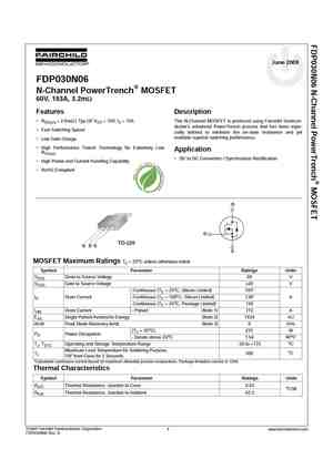
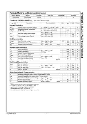
June 2009
FDP030N06
N-Channel PowerTrench MOSFET
60V, 193A, 3.2mΩ
Features Description
• RDS(on) = 2.6mΩ ( Typ.)@ VGS = 10V, ID = 75A This N-Channel MOSFET is produced using Fairchild Semicon-
ductor’s advanced PowerTrench process that has been espe-
• Fast Switching Speed
cially tailored to minimize the on-state resistance and yet
maintain superior switching performance.
1.2. fdp030n06b f102.pdf Size:641K _fairchild_semi

November 2013
FDP030N06B_F102
N-Channel PowerTrench MOSFET
60 V, 195 A, 3.1 mΩ
Features Description
• RDS(on) = 2.67 mΩ (Typ.) @ VGS = 10 V, ID = 100 A This N-Channel MOSFET is produced using Fairchild Semicon-
ductor’s advanced PowerTrench process that has been tai-
• Low FOM RDS(on) * QG
lored to minimize the on-state resistance while maintaining
superior switching perfor
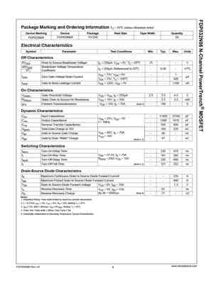
5.1. fdp032n08b.pdf Size:669K _fairchild_semi

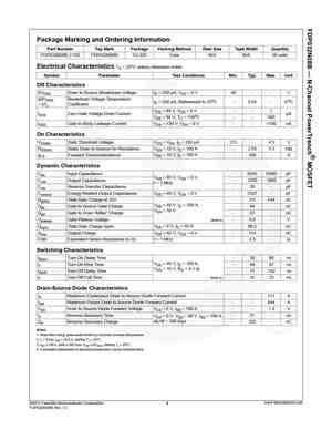
November 2013
FDP032N08B
N-Channel PowerTrench MOSFET
80 V, 211 A, 3.3 mΩ
Features Description
• RDS(on) = 2.85 mΩ (Typ.) @ VGS = 10 V, ID = 50 A This N-Channel MOSFET is produced using Fairchild Semicon-
ductor’s advanced PowerTrench process that has been tai-
• Low FOM RDS(on) * QG
lored to minimize the on-state resistance while maintaining
superior switching performance.
5.2. fdp032n08.pdf Size:619K _fairchild_semi
July 2008
FDP032N08
tm
N-Channel PowerTrench MOSFET
75V, 235A, 3.2mΩ
Features Description
• RDS(on) = 2.5mΩ ( Typ.)@ VGS = 10V, ID = 75A This N-Channel MOSFET is produced using Fairchild Semicon-
ductor’s adcanced PowerTrench process that has been espe-
• Fast switching speed
cially tailored to minimize the on-state resistance and yet
• Low gate charge
maintain superi
5.3. fdp036n10a.pdf Size:247K _fairchild_semi
July 2011
FDP036N10A
tm
N-Channel PowerTrench MOSFET
100V, 214A, 3.6mΩ
Features Description
• RDS(on) = 3.2mΩ ( Typ.)@ VGS = 10V, ID = 75A This N-Channel MOSFET is produced using Fairchild Semicon-
ductor’s advanced PowerTrench process that has been espe-
• Fast Switching Speed
cially tailored to minimize the on-state resistance and yet
maintain superior switching performa
5.4. fdp039n08b.pdf Size:691K _fairchild_semi

November 2013
FDP039N08B
N-Channel PowerTrench MOSFET
80 V, 171 A, 3.9 mΩ
Features Description
• RDS(on) = 3.16 mΩ (Typ.) @ VGS = 10 V, ID = 100 A This N-Channel MOSFET is produced using Fairchild Semicon-
ductor’s advanced PowerTrench process that has been tai-
• Low FOM RDS(on) * QG
lored to minimize the on-state resistance while maintaining
superior switching performance
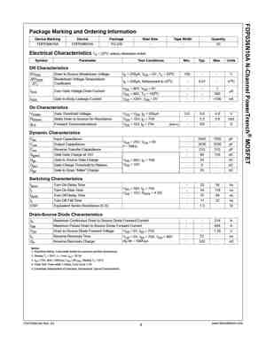
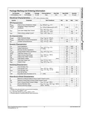
5.5. fdp038an06a0 fdi038an06a0.pdf Size:332K _fairchild_semi
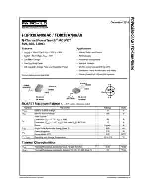
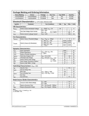
December 2010
FDP038AN06A0 / FDI038AN06A0
N-Channel PowerTrench MOSFET
60V, 80A, 3.8mΩ
Features Applications
• rDS(ON) = 3.5mΩ (Typ.), VGS = 10V, ID = 80A • Motor / Body Load Control
• Qg(tot) = 95nC (Typ.), VGS = 10V • ABS Systems
• Low Miller Charge • Powertrain Management
• Low QRR Body Diode • Injection Systems
• UIS Capability (Single Pulse and Repetitive P
Другие MOSFET… FDN372S
, STM4880
, FDN5618P
, FDN5630
, FDN8601
, STM4840
, FDN86246
, FDP025N06
, IRFP150N
, FDP032N08
, FDP036N10A
, STM4639
, FDP038AN06A0
, FDP040N06
, FDP045N10A_F102
, STM4637
, FDP047N08
.
FQP32N20C Datasheet (PDF)
1.1. fqp32n20c fqpf32n20c.pdf Size:1208K _fairchild_semi
QFET
FQP32N20C/FQPF32N20C
200V N-Channel MOSFET
General Description Features
These N-Channel enhancement mode power field effect • 28A, 200V, RDS(on) = 0.082Ω @VGS = 10 V
transistors are produced using Fairchild’s proprietary, • Low gate charge ( typical 82.5 nC)
planar stripe, DMOS technology.
• Low Crss ( typical 185 pF)
This advanced technology has been especially tailo
4.1. fqp32n12v2 fqpf32n12v2.pdf Size:856K _fairchild_semi
QFET
FQP32N12V2/FQPF32N12V2
120V N-Channel MOSFET
General Description Features
These N-Channel enhancement mode power field effect • 32 A, 120V, RDS(on) = 0.05Ω @VGS = 10 V
transistors are produced using Fairchild’s proprietary, • Low gate charge ( typical 41 nC)
planar stripe, DMOS technology.
• Low Crss ( typical 70 pF)
This advanced technology has been especially tailor
WFP50N06 Datasheet (PDF)
1.1. wfp50n06c.pdf Size:586K _winsemi
WFP50N06C
WFP50N06C
WFP50N06C
WFP50N06C
Silicon N-Channel MOSFET
Silicon N-Channel MOSFET
Silicon N-Channel MOSFET
Silicon N-Channel MOSFET
Features
R (Max 23mΩ)@V =10V
■ DS(on) GS
■ Ultra-low Gate Charge(Typical 31nC)
■ Fast Switching Capability
■ 100%Avalanche Tested
■ Maximum Junction Temperature Range(150℃)
General Description
This Power MOSFET is produced usin
1.2. wfp50n06.pdf Size:585K _winsemi
WFP50N06
WFP50N06
WFP50N06
WFP50N06
Silicon N-Channel MOSFET
Silicon N-Channel MOSFET
Silicon N-Channel MOSFET
Silicon N-Channel MOSFET
Features
R (Max 22mΩ)@V =10V
■ DS(on) GS
■ Ultra-low Gate Charge(Typical 31nC)
■ Fast Switching Capability
■ 100%Avalanche Tested
■ Maximum Junction Temperature Range(150℃)
General Description
This Power MOSFET is produced using Wi
FTP08N06A Datasheet (PDF)
1.1. ftp08n06a.pdf Size:274K _update
FTP08N06A
N-Channel MOSFET Pb
Lead Free Package and Finish
Applications:
• Automotive
VDSS RDS(ON) (Max.) ID
• DC Motor Control
55V 8 mΩ 120A
• Class D Amplifier
• Uninterruptible Power Supply (UPS)
Features:
D
• RoHS Compliant
• Low ON Resistance
• Low Gate Charge
• Peak Current vs Pulse Width Curve
G
• Inductive Switching Curves
G
D
S
TO-220
Ordering I
1.2. ftp08n06a.pdf Size:274K _inpower_semi
FTP08N06A
N-Channel MOSFET Pb
Lead Free Package and Finish
Applications:
• Automotive
VDSS RDS(ON) (Max.) ID
• DC Motor Control
55V 8 mΩ 120A
• Class D Amplifier
• Uninterruptible Power Supply (UPS)
Features:
D
• RoHS Compliant
• Low ON Resistance
• Low Gate Charge
• Peak Current vs Pulse Width Curve
G
• Inductive Switching Curves
G
D
S
TO-220
Ordering I
4.1. ftp08n50 fta08n50.pdf Size:468K _ark-micro

FTP08N50/FTA08N50
500V N-Channel MOSFET
BVDSS RDS(ON) (Max.) ID
General Features
Low ON Resistance
500V 0.9Ω 8.0A
Low Gate Charge (typical 33nC)
Fast Switching
100% Avalanche Tested
RoHS Compliant/Lead Free
Applications
High Efficiency SMPS
Adaptor/Charger
Active PFC
LCD Panel Power
Ordering Information
Part Number Package Marking
FTP08N50 TO-
IRFP32N50K Datasheet (PDF)
1.1. irfp32n50k irfp32n50kpbf.pdf Size:175K _upd-mosfet
IRFP32N50K, SiHFP32N50K
Vishay Siliconix
Power MOSFET
FEATURES
PRODUCT SUMMARY
• Low Gate Charge Qg Results in Simple Drive
VDS (V) 500
Available
Requirement
RDS(on) (Ω)VGS = 10 V 0.135
RoHS*
• Improved Gate, Avalanche and Dynamic dV/dt
Qg (Max.) (nC) 190 COMPLIANT
Ruggedness
Qgs (nC) 59
• Fully Characterized Capacitance and Avalanche Voltage
Qgd (nC) 84
and Current
Con
1.2. irfp32n50k.pdf Size:94K _international_rectifier
PD — 94099A
IRFP32N50K
SMPS MOSFET
HEXFET Power MOSFET
Applications
Switch Mode Power Supply (SMPS)
VDSS RDS(on)typ. ID
Uninterruptible Power Supply
High Speed Power Switching 500V 0.135Ω 32A
Hard Switched and High Frequency
Circuits
Benefits
Low Gate Charge Qg results in Simple
Drive Requirement
Improved Gate, Avalanche and Dynamic
dv/dt Ruggedness
Fully Characterize
1.3. irfp32n50kpbf.pdf Size:202K _international_rectifier
PD — 95052
IRFP32N50KPbF
SMPS MOSFET
HEXFET Power MOSFET
AppIications
l Switch Mode Power Supply (SMPS)
VDSS RDS(on)typ. ID
l Uninterruptible Power Supply
l High Speed Power Switching
500V 0.135Ω 32A
l Hard Switched and High Frequency
Circuits
l Lead-Free
Benefits
l Low Gate Charge Qg results in Simple
Drive Requirement
l Improved Gate, Avalanche and Dynamic
dv/dt Ruggednes
1.4. irfp32n50ks.pdf Size:115K _international_rectifier
PD — 94360
IRFP32N50KS
SMPS MOSFET
HEXFET Power MOSFET
Applications
Switch Mode Power Supply (SMPS)
VDSS RDS(on)typ. ID
Uninterruptible Power Supply
High Speed Power Switching 500V 0.135Ω 32A
Hard Switched and High Frequency
Circuits
Benefits
Low Gate Charge Qg results in Simple
Drive Requirement
Improved Gate, Avalanche and Dynamic
dv/dt Ruggedness
Fully Characterize
1.5. irfp32n50k sihfp32n50k.pdf Size:170K _vishay
IRFP32N50K, SiHFP32N50K
Vishay Siliconix
Power MOSFET
FEATURES
PRODUCT SUMMARY
Low Gate Charge Qg Results in Simple Drive
VDS (V) 500
Available
Requirement
RDS(on) (?)VGS = 10 V 0.135
RoHS*
Improved Gate, Avalanche and Dynamic dV/dt
Qg (Max.) (nC) 190 COMPLIANT
Ruggedness
Qgs (nC) 59
Fully Characterized Capacitance and Avalanche Voltage
Qgd (nC) 84
and Current
Configuration
1.6. irfp32n50k.pdf Size:260K _inchange_semiconductor
INCHANGE Semiconductor
isc N-Channel MOSFET Transistor IRFP32N50K
·FEATURES
·With TO-247 packaging
·With low gate drive requirements
·Easy to drive
·100% avalanche tested
·Minimum Lot-to-Lot variations for robust device
performance and reliable operation
·APPLICATIONS
·Switching applications
·ABSOLUTE MAXIMUM RATINGS(T =25℃)
a
SYMBOL PARAMETER VALUE UNIT
V Drain-Source
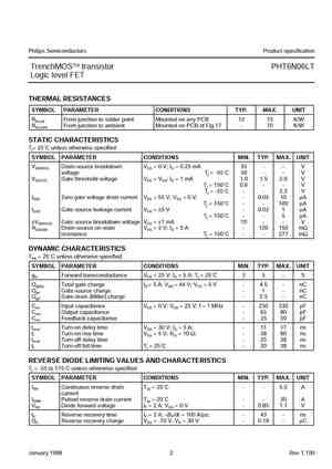
PHT6N06LT Datasheet (PDF)
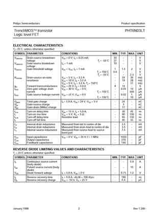
1.1. pht6n06lt 2.pdf Size:54K _philips
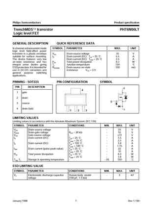

Philips Semiconductors Product specification
TrenchMOS transistor PHT6N06LT
Logic level FET
GENERAL DESCRIPTION QUICK REFERENCE DATA
N-channel enhancement mode SYMBOL PARAMETER MAX. UNIT
logic level field-effect power
transistor in a plastic envelope VDS Drain-source voltage 55 V
suitable for surface mounting. ID Drain current (DC) Tsp = 25 ˚C 5.5 A
The device features very low Dr
3.1. pht6n06t 1.pdf Size:58K _philips
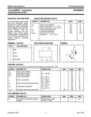
Philips Semiconductors Product specification
TrenchMOS transistor PHT6N06T
Standard level FET
GENERAL DESCRIPTION QUICK REFERENCE DATA
N-channel enhancement mode SYMBOL PARAMETER MAX. UNIT
logic level field-effect power
transistor in a plastic envelope VDS Drain-source voltage 55 V
suitable for surface mounting. ID Drain current (DC) Tsp = 25 ˚C 5.5 A
Using ’trench’ technology
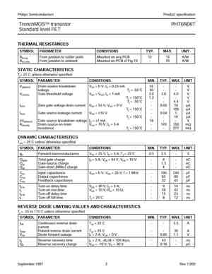
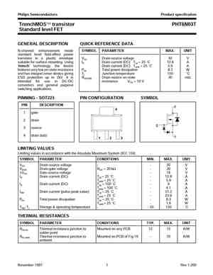
4.1. pht6n03lt 3.pdf Size:43K _philips
Philips Semiconductors Product specification
TrenchMOS transistor PHT6N03LT
Logic level FET
FEATURES SYMBOL QUICK REFERENCE DATA
• ’Trench’ technology VDSS = 30 V
d
• Very low on-state resistance
• Fast switching ID = 5.9 A
• Stable off-state characteristics
• High thermal cycling performance RDS(ON) ≤ 30 mΩ (VGS = 5 V)
g
• Surface mounting package
RDS(ON)
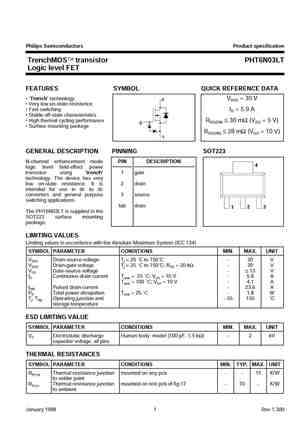
4.2. pht6n03t 2.pdf Size:57K _philips
Philips Semiconductors Product specification
TrenchMOS transistor PHT6N03T
Standard level FET
GENERAL DESCRIPTION QUICK REFERENCE DATA
N-channel enhancement mode SYMBOL PARAMETER MAX. UNIT
standard level field-effect power
transistor in a plastic envelope VDS Drain-source voltage 30 V
suitable for surface mounting. Using ID Drain current (DC) Tsp = 25 ˚C 12.8 A
’trench’ techno
MDF11N60TH Datasheet (PDF)
1.1. mdf11n60th.pdf Size:956K _magnachip
MDF11N60
N-Channel MOSFET 600V, 11A, 0.55Ω
General Description Features
The MDF11N60 uses advanced MagnaChip’s MOSFET V = 600V
DS
Technology, which provides low on-state resistance, high V = 660V @ T
DS jmax
switching performance and excellent quality. I = 11A @ V = 10V
D GS
R ≤ 0.55Ω @ V = 10V
DS(ON) GS
MDF11N60 is suitable device for SMPS, high Spee
3.1. mdf11n65b.pdf Size:781K _update
MDF11N65B
N-Channel MOSFET 650V, 12A, 0.65Ω
General Description Features
These N-channel MOSFET are produced using advanced VDS = 650V
MagnaChip’s MOSFET Technology, which provides low on- ID = 12A @ VGS = 10V
state resistance, high switching performance and excellent RDS(ON) ≤ 0.65Ω @ VGS = 10V
quality.
Applications
These devices are suitable device for SMPS, high Speed
3.2. mdf11n65b.pdf Size:781K _magnachip
MDF11N65B
N-Channel MOSFET 650V, 12A, 0.65Ω
General Description Features
These N-channel MOSFET are produced using advanced VDS = 650V
MagnaChip’s MOSFET Technology, which provides low on- ID = 12A @ VGS = 10V
state resistance, high switching performance and excellent RDS(ON) ≤ 0.65Ω @ VGS = 10V
quality.
Applications
These devices are suitable device for SMPS, high Speed
3.3. mdf11n65bth.pdf Size:781K _magnachip
MDF11N65B
N-Channel MOSFET 650V, 12A, 0.65Ω
General Description Features
These N-channel MOSFET are produced using advanced VDS = 650V
MagnaChip’s MOSFET Technology, which provides low on- ID = 12A @ VGS = 10V
state resistance, high switching performance and excellent RDS(ON) ≤ 0.65Ω @ VGS = 10V
quality.
Applications
These devices are suitable device for SMPS, high Speed
STP100N8F6 Datasheet (PDF)
1.1. stp100n8f6.pdf Size:535K _upd-mosfet
STP100N8F6
N-channel 80 V, 0.008 Ω typ., 100 A, STripFET F6
Power MOSFET in a TO-220 package
Datasheet — production data
Features
TAB
Order code VDS RDS(on)max ID PTOT
STP100N8F6 80 V 0.009 Ω 100A 176 W
• Very low on-resistance
• Very low gate charge
3
2
• High avalanche ruggedness
1
• Low gate drive power loss
TO-220
Applications
• Switching applications
F
1.2. stp100n8f6.pdf Size:205K _inchange_semiconductor
INCHANGE Semiconductor
Isc N-Channel MOSFET Transistor STP100N8F6
·FEATURES
·Very low on-resistance
·Very low gate charge
·High avalanche ruggedness
·Low gate drive power loss
·100% avalanche tested
·Minimum Lot-to-Lot variations for robust device
performance and reliable operation
·APPLICATIONS
·Switching applications
·ABSOLUTE MAXIMUM RATINGS(T =25℃)
a
SYMBOL PARAMET
3.1. stp100n10f7.pdf Size:1657K _upd-mosfet
STB100N10F7, STD100N10F7,
STF100N10F7, STP100N10F7
N-channel 100 V, 0.0068 Ω typ., 80 A, STripFET VII DeepGATE
Power MOSFET in D2PAK, DPAK, TO-220FP and TO-220
Datasheet — production data
Features
TAB TAB
RDS(on)
3
Order codes VDS max ID PTOT
1
3
1 DPAK
STB100N10F7 80 A 120 W
D2PAK
STD100N10F7 80 A 120W
TAB
100 V 0.008 Ω
STF100N10F7 45 A 30 W
STP100N10F7 80A 150 W
3.2. stp100n6f7.pdf Size:493K _update-mosfet
STP100N6F7
N-channel 60 V, 4.7 mΩ typ.,100 A STripFET F7
Power MOSFET in a TO-220 package
Datasheet — production data
Features
Order code VDS RDS(on) max. ID PTOT
STP100N6F7 60 V 5.6 mΩ 100A 125 W
TAB
• Among the lowest RDS(on) on the market
3
• Excellent figure of merit (FoM)
2
1
• Low Crss/Ciss ratio for EMI immunity
TO-220
• High avalanche ruggedness
Applicati
3.3. stp100nf04l.pdf Size:268K _update-mosfet
STP100NF04L
N-CHANNEL 40V — 0.0036 Ω — 100A TO-220
STripFET II POWER MOSFET
TYPE VDSS RDS(on) ID
STP100NF04L 40 V 3.4. stb100nf03l-03 stb100nf03l-03-1 stp100nf03l-03.pdf Size:460K _st
STP100NF03L-03
STB100NF03L-03 STB100NF03L-03-1
N-channel 30V — 0.0026? — 100A — D2PAK/I2/TO-220
STripFET III Power MOSFET
General features
Type VDSS RDS(on) ID
STB100NF03L-03 30V
3.5. stb100nf04 stp100nf04.pdf Size:398K _st
STP100NF04
STB100NF04
N-channel 40V — 0.0043? — 120A — TO-220 — D2PAK
STripFET II Power MOSFET
General features
Type VDSS RDS(on) ID Pw
STP100NF04 40V 3.6. stp100nf04l.pdf Size:268K _st
STP100NF04L
N-CHANNEL 40V — 0.0036 ? — 100A TO-220
STripFET II POWER MOSFET
TYPE VDSS RDS(on) ID
STP100NF04L 40 V 3.7. stp100n10f7.pdf Size:205K _inchange_semiconductor
INCHANGE Semiconductor
Isc N-Channel MOSFET Transistor STP100N10F7
·FEATURES
·Very low on-resistance
·Very low gate charge
·100% avalanche tested
·Minimum Lot-to-Lot variations for robust device
performance and reliable operation
·APPLICATIONS
·Switching applications
·ABSOLUTE MAXIMUM RATINGS(T =25℃)
a
SYMBOL PARAMETER VALUE UNIT
V Drain-Source Voltage 100 V
DSS
V Gate-
CMP80N06 Datasheet (PDF)
1.1. cmp80n06 cmb80n06 cmi80n06.pdf Size:1054K _update-mosfet
CMP80N06/CMB80N06/CMI80N06
N-Channel Enhancement Mode Field Effect Transistor
General Description Product Summery
The 80N06 is N-ch MOSFET
BVDSS RDSON ID
with extreme high cell density ,
60V 7.8m 80A
which provide excellent RDSON
and gate charge for most of the
Applications
synchronous buck converter
Motor Control
applications.
DC-DC converters
General Purpose Power Amplif
1.2. cmp80n06 cmb80n06 cmi80n06.pdf Size:1054K _cmos
CMP80N06/CMB80N06/CMI80N06
N-Channel Enhancement Mode Field Effect Transistor
General Description Product Summery
The 80N06 is N-ch MOSFET
BVDSS RDSON ID
with extreme high cell density ,
60V 7.8m 80A
which provide excellent RDSON
and gate charge for most of the
Applications
synchronous buck converter
Motor Control
applications.
DC-DC converters
General Purpose Power Amplif
IXFN32N60 Datasheet (PDF)
1.1. ixfk32n60 ixfn32n60 ixfk36n60 ixfn36n60.pdf Size:192K _ixys
IXFK 32N60 IXFN 32N60
IXFK 36N60 IXFN 36N60
Preliminary Data
VDSS ID25 RDS(on) trr
IXFK/FN 36N60 600V 36A 0.18Ω 250ns
HiPerFETTM Power MOSFET
IXFK/FN 32N60 600V 32A 0.25Ω 250ns
N-Channel Enhancement Mode
Avalanche Rated, High dv/dt, Low trr
TO-264 AA (IXFK)
Symbol Test Conditions Maximum Ratings
IXFK IXFN
VDSS TJ = 25°C to 150°C 600 600 V
G
VDGR TJ = 25°C to 150°C; RGS = 1
5.1. ixfn39n90.pdf Size:128K _ixys
VDSS = 900 V
IXFN 39N90
HiPerFETTM
ID25 = 39 A
Power MOSFETs
Ω
RDS(on) = 0.22 Ω
Ω
Ω
Ω
Single MOSFET Die
D
≤
trr ≤
≤ 250 ns
≤
≤
N-Channel Enhancement Mode
G
Avalanche Rated, High dv/dt, Low t
rr
S
S
Symbol Test Conditions Maximum Ratings
miniBLOC, SOT-227 B (IXFN)
VDSS TJ = 25°C to 150°C 900 V
E153432
VDGR TJ = 25°C to 150°C; RGS = 1 MΩ 900
5.2. ixfn34n80.pdf Size:128K _ixys
HiPerFETTM Power MOSFETs
IXFN 34N80 VDSS = 800 V
Single DieMOSFET
ID25 = 34 A
RDS(on) = 0.24 W
N-Channel Enhancement Mode D
Avalanche Rated, High dv/dt, Low trr
trr £ 250 ns
Preliminary data sheet
S
Symbol Test Conditions Maximum Ratings miniBLOC, SOT-227 B
E153432
VDSS TJ = 25°C to 150°C 800 V
S
VDGR TJ = 25°C to 150°C; RGS = 1 MW 800 V
G
VGS Continuous ±20 V
VGSM Transi
5.3. ixfn340n07.pdf Size:104K _ixys
HiPerFETTM
IXFN 340N07 VDSS = 70 V
Power MOSFETs
ID25 = 340 A
Ω
Ω
Single Die MOSFET RDS(on) = 4 mΩ
Ω
Ω
D
≤
trr ≤
≤ 200 ns
≤
≤
N-Channel Enhancement Mode
G
Avalanche Rated, High dv/dt, Low trr
S
S
Symbol Test Conditions Maximum Ratings miniBLOC, SOT-227 B (IXFN)
E153432
VDSS TJ = 25°C to 150°C70 V
S
VDGR TJ = 25°C to 150°C; RGS = 1 MΩ 70 V
G
VGS Co
5.4. ixfn36n100.pdf Size:128K _ixys
HiPerFETTM
IXFN 36N100 V = 1000V
DSS
Power MOSFETs
ID25 = 36A
Ω
Ω
Single Die MOSFET RDS(on) = 0.24Ω
Ω
Ω
D
N-Channel Enhancement Mode
G
Avalanche Rated, High dv/dt, Low t
rr
S
S
Symbol Test Conditions Maximum Ratings
miniBLOC, SOT-227 B (IXFN)
E153432
VDSS TJ = 25°C to 150°C 1000 V
S
VDGR TJ = 25°C to 150°C; RGS = 1 MΩ 1000 V
G
VGS Continuous ±20 V
VGSM
5.5. ixfn34n100.pdf Size:570K _ixys
IXFN 34N100 VDSS = 1000V
HiPerFETTM
ID25 = 34A
Power MOSFETs
Ω
RDS(on) = 0.28Ω
Ω
Ω
Ω
Single Die MOSFET
D
N-Channel Enhancement Mode
Avalanche Rated, High dv/dt, Low trr G
S
S
Symbol Test Conditions Maximum Ratings
miniBLOC, SOT-227 B (IXFN)
E153432
VDSS TJ = 25°C to 150°C 1000 V
S
VDGR TJ = 25°C to 150°C; RGS = 1 MΩ 1000 V
G
VGS Continuous ±20 V
VGSM Tran
FQP32N12V2 Datasheet (PDF)
1.1. fqp32n12v2 fqpf32n12v2.pdf Size:856K _fairchild_semi
QFET
FQP32N12V2/FQPF32N12V2
120V N-Channel MOSFET
General Description Features
These N-Channel enhancement mode power field effect • 32 A, 120V, RDS(on) = 0.05Ω @VGS = 10 V
transistors are produced using Fairchild’s proprietary, • Low gate charge ( typical 41 nC)
planar stripe, DMOS technology.
• Low Crss ( typical 70 pF)
This advanced technology has been especially tailor
4.1. fqp32n20c fqpf32n20c.pdf Size:1208K _fairchild_semi
QFET
FQP32N20C/FQPF32N20C
200V N-Channel MOSFET
General Description Features
These N-Channel enhancement mode power field effect • 28A, 200V, RDS(on) = 0.082Ω @VGS = 10 V
transistors are produced using Fairchild’s proprietary, • Low gate charge ( typical 82.5 nC)
planar stripe, DMOS technology.
• Low Crss ( typical 185 pF)
This advanced technology has been especially tailo
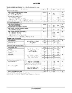
NTD32N06LG Datasheet (PDF)
1.1. ntd32n06l ntd32n06lg.pdf Size:98K _update-mosfet
NTD32N06L
Power MOSFET
32 Amps, 60 Volts
Logic Level, N-Channel DPAK
Designed for low voltage, high speed switching applications in
http://onsemi.com
power supplies, converters and power motor controls and bridge
circuits.
VDSS RDS(ON) TYP ID MAX
Features
• Smaller Package than MTB30N06VL
60 V
23.7 mW
32 A
• Lower RDS(on), VDS(on), and Total Gate Charge
• Lower and Tighter
1.2. ntd32n06l ntd32n06l ntd32n06lg.pdf Size:98K _onsemi
NTD32N06L
Power MOSFET
32 Amps, 60 Volts
Logic Level, N-Channel DPAK
Designed for low voltage, high speed switching applications in
http://onsemi.com
power supplies, converters and power motor controls and bridge
circuits.
VDSS RDS(ON) TYP ID MAX
Features
• Smaller Package than MTB30N06VL
60 V
23.7 mW
32 A
• Lower RDS(on), VDS(on), and Total Gate Charge
• Lower and Tighter
2.1. ntd32n06-001 ntd32n06.pdf Size:66K _update-mosfet
NTD32N06
Power MOSFET
32 Amps, 60 Volts, N-Channel DPAK
Designed for low voltage, high speed switching applications in
power supplies, converters and power motor controls and bridge
circuits.
http://onsemi.com
Features
• Pb-Free Packages are Available
V(BR)DSS RDS(on) TYP ID MAX
• Smaller Package than MTB36N06V
60 V 26 mW 32 A
• Lower RDS(on)
• Lower VDS(on)
N-Channel
•
2.2. ntd32n06-001 ntd32n06 ntd32n06-d.pdf Size:66K _onsemi
NTD32N06
Power MOSFET
32 Amps, 60 Volts, N-Channel DPAK
Designed for low voltage, high speed switching applications in
power supplies, converters and power motor controls and bridge
circuits.
http://onsemi.com
Features
• Pb-Free Packages are Available
V(BR)DSS RDS(on) TYP ID MAX
• Smaller Package than MTB36N06V
60 V 26 mW 32 A
• Lower RDS(on)
• Lower VDS(on)
N-Channel
•